801 Gerber Street, Ligonier, IN 46767-9907
Phone: 800-747-5749 • Fax: 260-894-4190
email: ame@metaletching.com

Data Sheet
Typical Photoetching Dimensions for Metal Specialties and Complex Metal Parts from Advanced Metal Etching
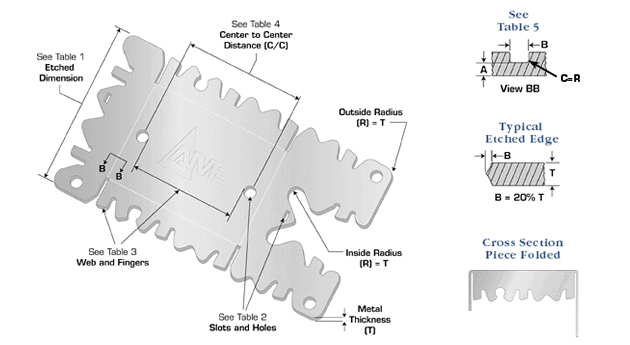
Table 1 Etched Dimension Tolerances |
||||||
|---|---|---|---|---|---|---|
Thickness (T) in inches |
||||||
.001" |
.002" |
.005" |
.010" |
.015" |
.020" |
.040" |
Empirical |
±.0010 |
±.0010 |
±.0015 |
±.0020 |
±.0030 |
±.0050 |
Table 2 Holes or Slots |
|
|---|---|
Metal Thickness (T) |
Diameter or Width |
.001" -0.005" |
At least Metal Thickness, Minimum .003" |
.005" or Over |
Minimum of 1.1 times Metal Thickness |
Table 3 Web or Finger |
|
|---|---|
Thickness (T) |
Space Between Holes (W) |
Less than .005" |
At least Metal Thickness, Minimum .003" |
Over .005" |
Minimum of 1.0 times Metal Thickness |
Table 4 Center to Center Tolerances |
|
|---|---|
C/C Dimensions (inches) |
Tolerance Attainable |
1.0" or Less |
±.0005" |
1.0" - 3.0" |
±.0010" |
3.0" - 6.0" |
±.0020" |
6.0" - 10.0" |
±.0030" |
Table 5 Half Etch Based on Material Thickness |
||
|---|---|---|
A |
B |
C |
25% - 75% |
100% + |
25% |
What is Photo Etching?
Photo Etching is also called metal etching, chemical etching, chemical milling, photo etching, chemical etching, photochemical machining, chemical machining.
Photo etching is a process used in the creation of integrated circuits, that combines photolithography with the etching process. Photolithography is used to form patterns on semiconductor substrates coated with photoresist, resulting in selective developing of the photo-resist, when exposed to ultra-violet light through a photomask. The substrate is then etched, during which process the developed photoresist serves as a barrier against the etchant, resulting in only the selected area being etched.